12 stage Cockroft-Walton voltage multiplier circuit
By Dominic-Luc Webb
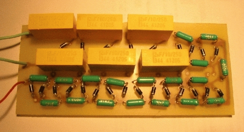


My time is limited at the moment. In a nutshell, the first three stages utilize six 12 uF 250 V caps (the big yellow ones) and the remaining stages use 47 nF 250 volt caps (small green ones). The diodes are 1N4007 throughout. The holes along the middle of the board are points at which I can solder in wires to draw current from each of the stages. I can easily get a pulsed square wave 10 volt DC supply as an input up to about 60 volts without noticable sag, drawing from the middle stages. The last several stages display pretty bad voltage sag; at this point, I don't think I need so many stages, so I won't bother worrying about the sag on these later stages. Sag at higher stages is a general problem of the C-W circuit. The input pulses originate from a 12 VDC battery driven 555 timer in a classical RC controlled astable multivibrator mode with frequency about 1 kHz and a roughly 65% duty cycle.
The complete circuit (a PMT power supply) will have the 555 timer driving 3 small transformers tied in parallel on the primary and in series on the secondary. The two ends of the serial tied secondaries will output to this CW circuit. The transformers are each about 15 mm square and resistance on the primary side is about 0.5 Ohm and on the secondary about 60 Ohm. The 555 output (pin 3) tied directly to the transformers can output 200-300 volts at the secondaries (again, outputs in serial), depending on how this is measured (due to voltage drop, meter used, etc). Given that a PMT such as the 931B cannot handle more than -1250 VDC, my circuit should be sufficient and it seems to be proving to be relatively robust and quite cheap. Part of my definition of robust, is easily and reproducibly built by a novice. Note that I need -1250 VDC (that is, minus 1250 VDC). I am thinking on how best to achieve the voltage inversion, but this should not be a big deal.
This was the easiest part of the circuit to build. The only noteworthy experience was that the solder connections need to be of good quality. I noticed some very bad sag on the 4th stage and that was immediately eliminated by some additional soldering at a joint that had less than 1 Ohm resistance, albeit this was more than the other joints. There were hurdles I had to overcome in the overall power supply circuit. Getting a transformer to generate a decent voltage amplification was a major one. The primary aim was to do photon counting (readout is counts per second) photometry using batteries, which fits well with my general goal of automated (robotic?) telescopes. A secondary aim was a high voltage circuit for a vacuum aluminizing rig. If one accepts gross power inefficiency, one has no problems, but if one wants to power a PMT from a battery that should last some time between recharging episodes, significant learning needs to be done about how transformers work, the different types, and how to tweak them to peak performance. I hope to write a lot about this in the future. Suffice it to say for now that the present circuit has the transformer experiencing a square wave with 65% duty cycle, and that diverting only a few percent from this translated into markedly reduced voltage amplification on the secondary side of the transformer. This obviously can transduce into poor PMT performance.
Another obstacle was understanding details of how NPN transistors are rated and how to apply and test them. There are circuits that drive step-up, high voltage (HV), coils or speakers from the 555 timer in which output pin 3 first goes to an NPN transistor base and the coil primary current goes through the collector. While I get this to work and to follow the basic transistor equations, like Beta = Ic/Ib, the coil performance was pretty much always cowardly in comparison to driving the coil directly from pin 3 and skipping the NPN. The 555 is itself no wimp and probably can drive the coils and PMT by itself. I plan for the PMT to be quite sensitive and operate well below 1 mA, so I am hoping the total power drawn from the 555 will be well below 500 mW. I nonetheless invested time in understanding how this NPN wimpiness comes about and how best to connect an NPN for PMT power supplies. I hope to write much about this as well.
As I get time, I will post equations, schematics, PCB layouts and oscilloscope traces, etc, which will go into the empty picture frames. For now, I need to end a 12 hour day in my lab. Please note that the newsgroup sci.electronics.basics was an invaluable resource and much intellectual guidance came from John Popelish whose time often resides within this newsgroup.
Regarding the etching of the board, I tinkered around with the chemistry of transfering a PCB layout from common overhead transparency to PCB copper and have met with greatly improved success. I am now getting very nice transfers that both transfer and stick well and protect the copper very nicely during the etching process even with shaking. I will perfect this procedure and post details later. Now that I understand the process, I need to build a simple rig to do the transfers.
Parts:
C1-C6 12 uF @ 250 V (type ???)
C7-C24 47 nF @ 250 V (type ???)
D1-D24 1N4007 1000 V @ 1.0 A
The remaining items relate to the circuit board:
1 overhead transparency
1 permanent marker
1 single sided PCB board
1 spoonful of ammonium persulphate
References
Dominic-Luc Webb > dlwebb@canit.se